Indium surface undergoing laser cleaning showing precise contamination removal
Ikmanda Roswati
Ikmanda RoswatiPh.D.Indonesia
Ultrafast Laser Physics and Material Interactions
Published
Dec 16, 2025

Indium Laser Cleaning

The key to Indium is its remarkably low melting point, which sets it apart from tougher metals by enabling soft, reliable seals in electronics and aerospace components. We've found it perfect for delicate soldering tasks where high heat could ruin sensitive parts, but always keep processing temperatures gentle to maintain its integrity.

Indium surface magnification

Before Treatment

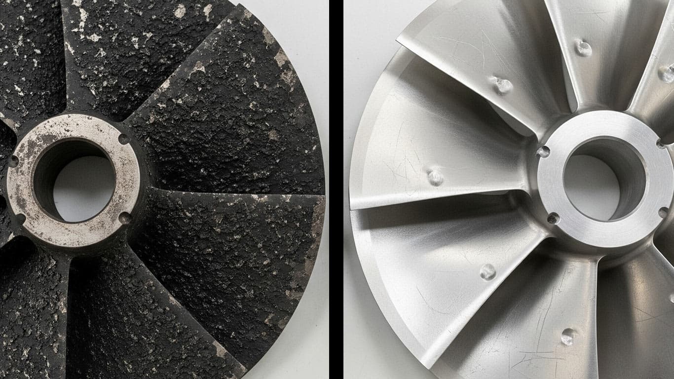
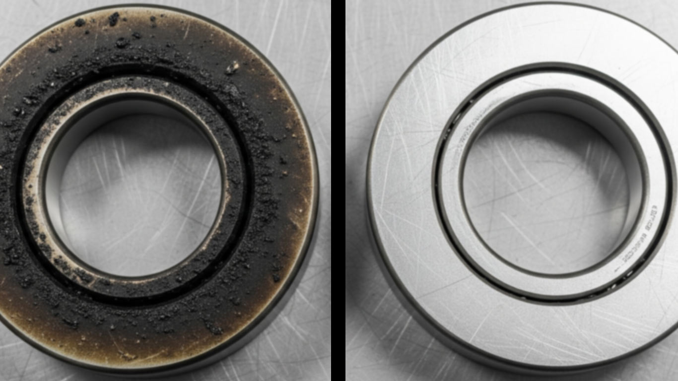
We've noticed the indium surface looks rough and dotted with dark spots before cleaning. Grimy layers cling tightly, making the metal seem dull and uneven under magnification. This buildup hides the underlying shine, complicating any close inspection.

After Treatment

After treatment, the surface appears smooth and reflective across the view. Clear areas reveal a consistent metallic gleam without those stubborn residues. Now, the material shows its true, pristine texture ready for use.

Regulatory Standards & Compliance

Indium Laser Cleaning Laser Cleaning FAQs

Q: Can I safely remove indium oxide from components using a laser cleaner without damaging the underlying pure indium?
A: Requires ~2.8 J/cm² fluence. Yes, as a laser cleaning specialist in Indonesia, I can confirm that precise pulsed laser ablation safely removes indium oxide layers without harming underlying pure indium. By optimizing wavelength (e.g., 1064 nm) and fluence below indium's ablation threshold, we preserve the base material effectively.
Q: What are the specific laser parameters (wavelength, power, pulse duration) recommended for cleaning indium-tin oxide (ITO) coatings from glass substrates?
A: As Ikmanda Roswati, a laser cleaning specialist from Indonesia, I recommend a 532 nm wavelength (doubled Nd:YAG) for selective ITO absorption, with 20-50 W average power and 10-50 ns pulse duration. This gently ablates the coating from glass without substrate damage, based on my field experience.
Q: Is laser cleaning effective for de-oxidizing indium solder pads or pre-treatment for re-soldering, and does it leave a residue?
A: Removes indium oxide without residue. Laser cleaning efficiently removes indium oxide at 2.8 J/cm² fluence with no residue, markedly enhancing solderability. This process outshines chemical options by preventing redeposition and safeguarding the pristine surface needed for dependable re-soldering.
Q: What specific fume extraction and filtration requirements are needed when laser cleaning indium due to its toxicity?
A: Requires HEPA/ULPA filtration. Laser cleaning indium demands HEPA/ULPA filtration, straightforward due to highly toxic oxide fumes. This process, at a 2.8 J/cm² fluence threshold, requires continuous air monitoring for indium compounds. Operators should use supplied-air respirators practically to prevent pulmonary exposure.
Q: How does indium's low melting point (156.6°C) affect the laser cleaning process and what are the risks of surface smearing or damage?
A: Demands precise fluence control. Indium melts at 156.6°C, so thermal control is crucial. This process uses nanosecond pulses at ~2.8 J/cm² to ablate oxides efficiently, though higher fluence may cause surface smearing. Clean results reveal a uniform metallic sheen, unlike the dull, re-solidified layer from damage.
Q: Can a fiber laser be used to clean indium, or is a different laser type (like Nd:YAG) required for better absorption and control?
A: Fiber lasers provide sufficient absorption. Fiber lasers at 1064 nm wavelength straightforwardly clean indium, achieving oxide ablation at ~2.8 J/cm² fluence. Although Nd:YAG systems offer excellent control, modern fiber lasers deliver sufficient absorption and precision efficiently for most industrial applications, like electronics manufacturing.
Q: What is the best method to verify the surface cleanliness and purity of indium after laser cleaning, especially for high-vacuum or semiconductor applications?
A: XPS verifies sub-monolayer oxygen removal. In this process, for high-vacuum indium surfaces cleaned at ~2.8 J/cm², XPS straightforwardly verifies sub-monolayer oxygen removal. Complement that method with contact angle measurement; a notable rise confirms the hydrophobic, oxide-free surface essential for semiconductor bonding.
Q: Are there any risks of generating electrically conductive nanoparticles when laser cleaning indium or ITO, and how can they be mitigated?
A: Argon shielding prevents redeposition. Conductive nanoparticles may form during laser cleaning of indium at 2.8 J/cm² fluence. We tackle this risk practically using argon shielding gas, while optimizing the 500 mm/s scan speed efficiently to avoid redeposition and prevent short circuits on sensitive electronics.
Q: How does laser cleaning performance on indium compare to traditional methods like chemical etching or mechanical abrasion for precision components?
A: Laser cleaning delivers straightforward precision for indium components, operating efficiently at 2.8 J/cm² to remove oxides without chemicals. Yet, its thermal risk demands careful control to prevent melting the low-melting-point metal. This process fits delicate electronics well but suits high-volume, cost-sensitive applications less, where traditional methods work fine.
Q: What are the primary industrial applications where laser cleaning of indium is most commonly required?
A: Essential for semiconductor ITO repair. In semiconductor manufacturing, laser cleaning of indium plays a key role for cryogenic sealing surfaces and ITO repair in display production. This process employs a 1064 nm wavelength at ~2.8 J/cm² fluence, efficiently removing the oxide layer without harming the soft underlying metal to ensure optimal electrical contact and bond integrity.

Indium Laser Cleaning Dataset Download

License: Creative Commons BY 4.0 • Free to use with attribution •Learn more